




An OLED panel is not a single sheet of light-emitting material. It is a carefully arranged stack containing a substrate, TFT circuits, electrodes, organic functional layers, and protective encapsulation.
Each part has a specific purpose. Some components support the panel, some generate and control light, and others protect the OLED materials from the environment. Changing these components also makes rigid, flexible, and transparent OLED panels possible.
This article looks inside the physical structure of an OLED panel. To learn how electrical signals control the pixels and create an image, read How Does an OLED Display Work?.
From an Image to an OLED Element
An image or video on an OLED display is formed by millions of pixels arranged across the screen.
Each pixel is generally made up of red, green, and blue subpixels. By changing the brightness of these three colors, the display produces the required color for each pixel.
Inside every subpixel are two connected parts:
- An OLED element that produces colored light
- A TFT transistor that regulates its electrical current and brightness
In simple terms:
Image → Pixels → RGB Subpixels → OLED Element + TFT
The OLED element and TFT do not sit alone. They are built into a larger layer stack that supports, drives, and protects the complete pixel array.
The Basic OLED Layer Stack
A simplified OLED display structure may contain eight main layers, arranged from bottom to top:
- Substrate
- TFT backplane
- Anode
- Hole injection and transport layers
- Emissive Layer (EML)
- Electron transport and injection layers
- Cathode
- Encapsulation
These layers can be divided into three groups. The substrate and TFT backplane provide support and driving circuitry. The two electrodes and organic layers form the OLED element. Encapsulation protects the active materials.
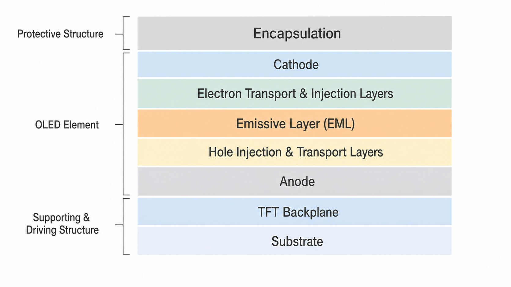
Commercial panels may include additional transport, blocking, optical, or emissive layers. However, this simplified stack is enough to understand the main OLED display structure.
Substrate and TFT Backplane
Everything begins with the substrate, which provides the surface on which the TFT backplane and OLED elements are formed.
Glass provides a flat and stable base for a rigid OLED panel, while a suitable polymer substrate allows a flexible panel to bend. The substrate therefore influences the panel’s thickness, stability, transparency, and flexibility.
Formed on the substrate, the TFT backplane contains thin-film transistors, storage capacitors, conductive lines, and electrical contacts. Each subpixel is connected to this driving circuitry, which regulates the current supplied to its OLED element.
In simple terms, the substrate supports the panel, while the TFT backplane provides the electrical control needed for each subpixel.
Electrodes and OLED Emission Direction
The anode and cathode sit on opposite sides of the organic functional layers. The anode provides the interface for holes to enter the organic stack, while the cathode provides the interface for electrons.
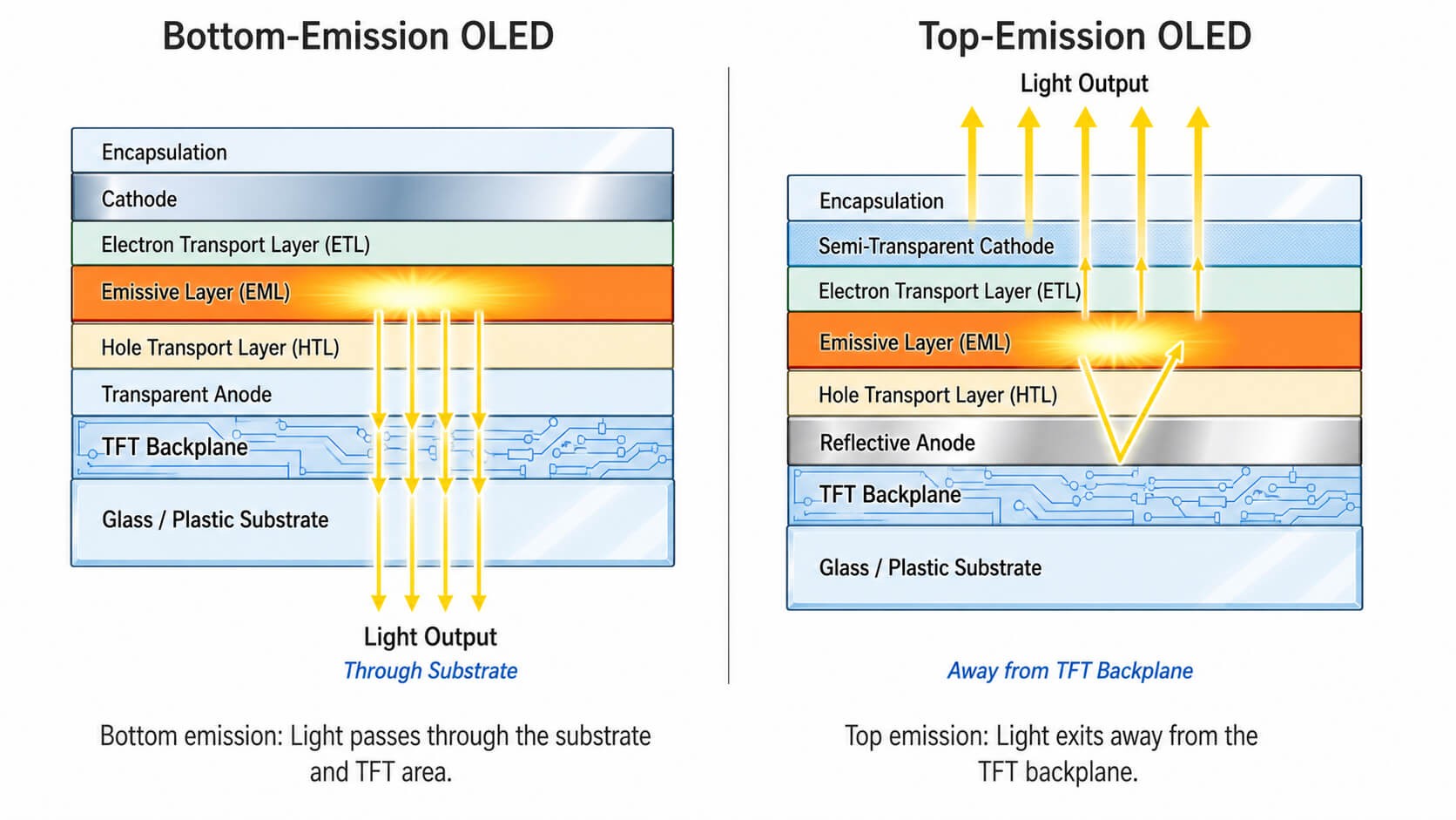
But these electrodes do more than conduct electricity. They also help determine the direction in which light leaves the OLED panel. Depending on the design, an electrode can be transparent, semi-transparent, or reflective.
Bottom-Emission OLED
A bottom-emission OLED generally uses a transparent anode below the organic layers and a reflective cathode above them.
Light generated in the Emissive Layer travels toward the anode and exits through the TFT-backplane and substrate side. The cathode reflects some of the light travelling in the opposite direction back toward this path.
Because the TFT circuitry is located in the light path, it can reduce the available transmitting area.
Top-Emission OLED
A top-emission OLED reverses this optical arrangement. It generally uses a reflective anode below the organic layers and a transparent or semi-transparent cathode above them.
The reflective anode directs light away from the substrate. Light then exits through the upper cathode and encapsulation without passing through the TFT backplane.
Keeping the backplane outside the primary light path can provide more usable emitting area, particularly when the pixel contains dense driving circuitry.
“Top” and “bottom” describe the direction of light relative to the substrate. They do not refer to the way the finished screen is positioned after installation.
What Are the Organic Layers?
The term organic layers can be misleading because it sounds like one layer. In practice, it refers to several extremely thin functional layers placed between the anode and cathode.
| Layer | Main role |
|---|---|
| Hole Injection Layer (HIL) | Helps holes enter from the anode |
| Hole Transport Layer (HTL) | Moves holes toward the EML |
| Emissive Layer (EML) | Contains the light-emitting material |
| Electron Transport Layer (ETL) | Moves electrons toward the EML |
| Electron Injection Layer (EIL) | Helps electrons enter from the cathode |
Electrons and holes travel from opposite sides and meet in the EML, where their energy is released as light. The emissive material helps determine the color of that light.
Only these functional parts of the panel use organic light-emitting and transport materials. Despite the name “OLED,” the entire display is not organic. Its substrate, TFT backplane, electrodes, electrical connections, and encapsulation use other types of materials.
Encapsulation and Edge Sealing
OLED materials are sensitive to moisture and oxygen. Without protection, exposure to the environment can gradually damage the active layers.
Encapsulation forms a barrier over the OLED structure, while edge sealing protects the perimeter of the active area.
Rigid panels can use a glass-based protective structure. Panels designed to bend generally require Thin-Film Encapsulation (TFE), which uses thin barrier layers instead of a rigid sealing plate.
If this protection is damaged, dark spots, edge darkening, uneven output, or progressive pixel failure may appear. However, similar symptoms can also be caused by connection problems, damaged driver components, or physical impact.
Rigid, Flexible and Transparent OLED Structures
Rigid, flexible, and transparent OLEDs use the same basic light-emitting principle. Their differences come from how the substrate, encapsulation, electrodes, and pixel areas are designed.

Rigid OLED
A rigid OLED generally uses a glass substrate and a fixed protective structure. The result is a flat and mechanically stable panel that is not intended to bend after assembly.
Flexible OLED
A flexible OLED display uses a polymer substrate together with a compatible backplane, electrodes, connections, and thin-film encapsulation.
However, “flexible” does not always mean freely foldable. Some panels are designed for one fixed curve. A repeatedly foldable display requires every part of the panel and surrounding structure to withstand that movement.
Transparent OLED
A transparent OLED display uses light-transmitting materials and divides its pixel layout into two areas:
- Active areas that generate the image
- Transmissive areas through which the background remains visible
Making more space transparent leaves less room for OLED elements and TFT circuitry. A transparent OLED must therefore balance transparency with emitting area, pixel density, brightness, and image visibility.
OLED Material Summary
An OLED panel combines several material categories:
| Component | Common material category |
|---|---|
| Substrate | Glass or heat-resistant polymer |
| TFT backplane | Semiconductor, insulating, and conductive materials |
| Electrodes | Metallic or transparent conductive materials |
| Organic stack | Injection, transport, and emissive materials |
| Encapsulation | Glass or multilayer barrier films |
| Edge seal | Barrier adhesive or sealing material |
The exact materials and layer designs vary between panels. Specifications should therefore be checked for the actual product rather than assumed from the general term “OLED.”
Conclusion
An OLED display is a coordinated multilayer structure. The substrate provides the foundation, the TFT backplane carries the pixel-driving circuits, the electrodes and organic layers form the light-emitting elements, and encapsulation protects the sensitive materials.
The electrode design determines whether light exits through the substrate side or away from the TFT backplane. Changes to the substrate, encapsulation, and pixel layout then make rigid, flexible, and transparent OLED panels possible.
Although these panels may look very different, they are all built around the same basic idea: millions of individually controlled OLED elements arranged within a thin, protected pixel structure.
FAQ
Are all layers in an OLED display organic?
No. Only the charge-injection, transport, and light-emitting layers use organic functional materials. The substrate, TFT backplane, electrodes, electrical connections, and encapsulation use glass, polymers, metals, semiconductors, and other materials.
What is the difference between an OLED element and an OLED subpixel?
The OLED element is the light-emitting structure formed by the electrodes and organic layers. A subpixel includes this OLED element together with its associated TFT driving circuit. The OLED element generates colored light, while the TFT controls its brightness.
Is a flexible OLED display always foldable?
No. Some flexible OLED panels are designed for a fixed curve rather than repeated folding. A foldable display requires the substrate, TFT backplane, electrodes, encapsulation, connections, protective layers, and surrounding structure to tolerate repeated movement.