




An LCD screen begins as raw sheets of glass. By depositing microscopic switching circuits on one substrate, forming color filters on another, and sealing a cell of liquid crystal between them, manufacturers create the screen's core light-modulating engine. Adding polarizers, driver electronics, and a backlight then transforms this physical stack into a functional display module.
Industrially, these operations fall into three overarching phases—array fabrication, cell assembly, and module integration—executed across several distinct production stages:
The LCD Manufacturing Process at a Glance
| Stage | What happens | What it creates |
| Glass preparation | Large glass sheets are cleaned and inspected | Clean, stable surfaces for precision processing |
| TFT array & CF fabrication | Circuits and RGB filters are formed on separate substrates | Electrical switching and color-control structures |
| Cell assembly | Alignment layers, spacers, sealant, and liquid crystal are joined | A sealed liquid crystal cell |
| Panel separation | Large mother glass is divided into individual panels | Sized panels ready for module assembly |
| Module assembly | Polarizers, drivers, backlight, and frames are integrated | A functional LCD module (LCM) |
| Inspection & testing | Electrical, optical, and environmental checks are performed | Verified modules ready for final display integration |
(To understand how these layers physically manipulate light, see how an LCD works. The guide below focuses strictly on how those structures are built and assembled.)
1. Preparing the Glass Substrates
LCD production begins with massive sheets known as mother glass, allowing factories to process multiple screens simultaneously rather than handling small panels one by one.
According to Corning’s glass-size comparison, Gen 8.5 glass measures approximately 2.2 × 2.5 meters, while a Gen 10.5 sheet expands to roughly 2.94 × 3.37 meters. Producing panels at this scale is primarily an economic calculation: how efficiently target screen sizes fit across the sheet dictates overall material utilization. A larger sheet format is only advantageous when panel dimensions align with it with minimal unused margin or scrap.
Once the layout and cutting efficiency are determined, the raw glass enters the processing line. Here, it undergoes thorough cleaning and inspection for surface scratches, micro-cracks, and airborne particles. A single microscopic speck can break a critical thin-film conductor or result in dead pixels inside the finished display.
Strict cleanroom protocols and electrostatic discharge (ESD) controls remain vital throughout this stage. With the glass surface verified and contamination-free, the substrate is ready for active thin-film deposition.
2. Building the TFT Array
The thin-film transistor (TFT) array serves as the screen’s electrical switching matrix, with dedicated transistors modulating the voltage across each subpixel's liquid crystal layer. Rather than mounting discrete components, manufacturers build these microscopic circuits directly onto the glass through sequential cycles of thin-film deposition, photolithography, and etching.
Depositing the Thin Films
Fabricating the backplane begins by laying down continuous, microscopic layers of conductive, insulating, and semiconductor materials across the entire substrate.
Sputtering—a physical vapor deposition (PVD) method—is typically used to deposit metal bus lines and transparent conductive films such as ITO. Meanwhile, plasma-enhanced chemical vapor deposition (PECVD) grows the critical dielectric layers (such as silicon nitride) and semiconductor channels (such as amorphous silicon). These unpatterned films provide the raw physical stack for the circuits that follow.
Patterning Films into Circuits
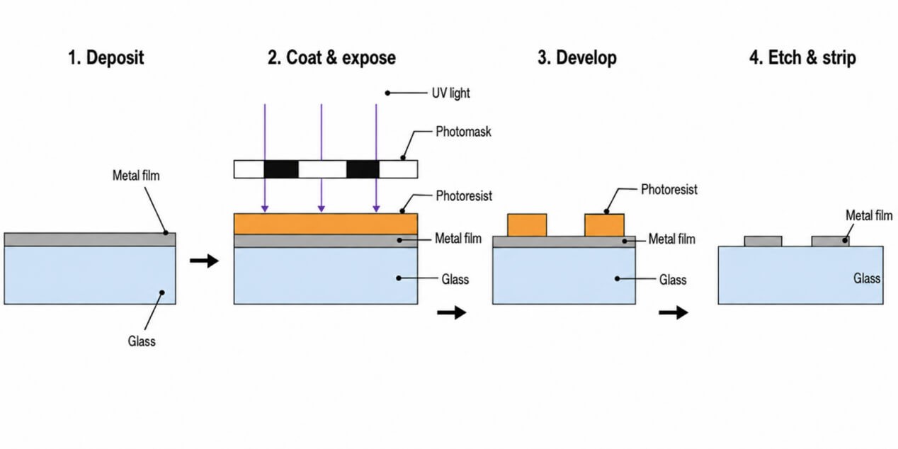
Once a film is deposited, photolithography transfers circuit geometry onto the glass. The surface is coated with photoresist, exposed to UV light through a precision photomask, and chemically developed to define protected regions. Subsequent wet or dry etching selectively strips away unwanted material, and the remaining photoresist is removed.
Repeating this cycle across multiple mask steps builds up the transistors, row/column addressing lines, and pixel storage electrodes layer by layer.
The ultimate performance of this circuit network depends heavily on the semiconductor material chosen for the transistor channel:
- Amorphous Silicon (a-Si): The industry workhorse, offering low cost and high manufacturability on massive glass substrates, but limited by lower electron mobility.
- Oxide Semiconductors (IGZO): Delivers substantially higher mobility and ultra-low off-state leakage current, making it well-suited for high-resolution panels and power-efficient static displays.
- Low-Temperature Polycrystalline Silicon (LTPS): Offers the highest electron mobility for ultra-compact transistors and high pixel densities, albeit at the expense of more complex processing and smaller substrate scalability.
Once the completed TFT substrate passes in-line array testing, it is ready to be paired with the opposing color filter substrate.
3. Making the Color Filter
While the TFT array forms the electrical switching network, the opposing substrate provides the screen’s color-filtering structure. Red, green, and blue filter regions align with individual subpixels, while a black matrix blocks light around their boundaries and over areas that should remain dark.
The colored layers are patterned onto the glass in successive steps. Their dimensions and positions must match the intended pixel layout: misplaced filter openings can reduce light transmission or allow unwanted light through neighboring regions.
Maintaining this registration across a large substrate requires precise exposure and dimensional control. Temperature changes and mask deformation can shift the pattern, so fabrication equipment uses alignment feedback and temperature control to maintain consistency across the sheet.
With both substrates prepared, production moves to cell assembly, where the liquid crystal layer is enclosed between them.
4. Assembling the Liquid Crystal Cell
Cell assembly turns two patterned substrates into a sealed optical structure. The process establishes the liquid crystal’s starting orientation, maintains a consistent separation between the glass surfaces, and fills the enclosed space without disrupting either.
Preparing the Alignment Layers
The inner surfaces receive a thin coating of alignment material, commonly based on polyimide (PI). Controlled coating and drying produce an even film, while baking removes residual solvent and develops the required material properties.
Rubbing or photoalignment gives the surface a preferred direction that guides the liquid crystal molecules. Rubbing uses controlled mechanical contact; photoalignment uses polarized light to modify a light-sensitive film. The coating, baking, and alignment sequence is selected around the material chemistry.
Uniform treatment helps the liquid crystal respond consistently across the panel. Local differences in the alignment layer can disturb that response and become visible as uneven brightness or light leakage.
Establishing the Cell Gap
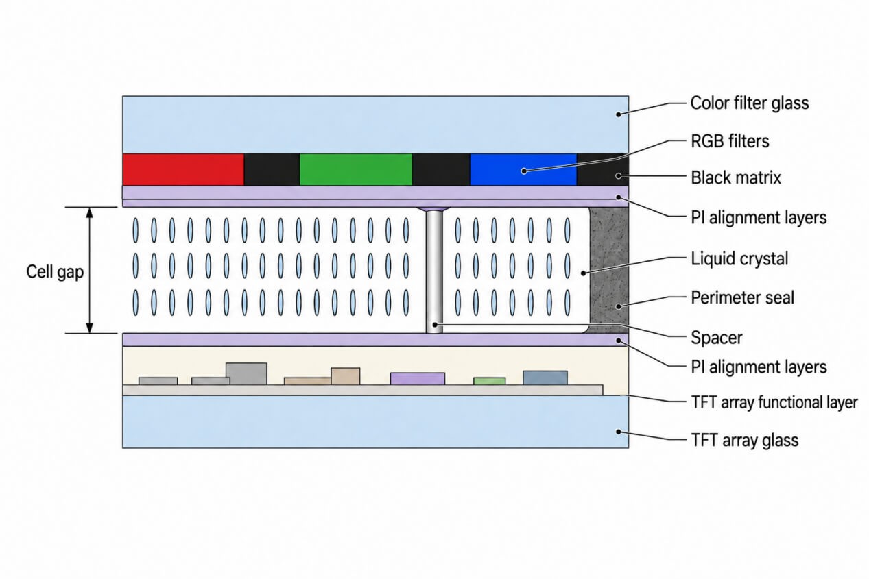
Spacers hold the substrates apart, creating a liquid crystal layer only a few micrometers thick. This separation—the cell gap—affects how the liquid crystal changes the light passing through it.
Viewed from the front of the display toward the backlight, the cell has the following simplified structure:
| Layer or feature | Role within the cell |
| Color filter glass and patterned layers | Support the RGB filters and black matrix |
| Upper alignment layer | Guide liquid crystal orientation at the upper surface |
| Liquid crystal layer | Modulate light in response to the electric field |
| Spacers distributed within the cell | Maintain the separation between the substrates |
| Lower alignment layer | Guide liquid crystal orientation at the lower surface |
| TFT array and glass substrate | Carry the switching circuits and pixel electrodes |
Simplified structure; electrode placement varies by LCD mode. Polarizers sit outside the cell.
Spacer height, substrate flatness, and assembly pressure work together to maintain an even gap. If the spacing varies, different regions can respond differently to the same driving signal, producing visible non-uniformity.
Filling and Sealing the Cell
Liquid crystal enters the assembly through one of two main routes.
In vacuum injection, the substrates are joined first, leaving a filling port in the perimeter seal. The empty cell is evacuated, filled through this opening, and then sealed. As panel dimensions increase, moving liquid crystal through the narrow internal gap takes longer.
One-drop filling (ODF) changes the sequence. A measured quantity of liquid crystal is dispensed onto a substrate before the two halves are aligned and joined under vacuum. The material spreads across the enclosed area as the substrates come together, avoiding the long filling path from a peripheral inlet.
Accurate dispensing and a continuous perimeter seal are essential to this process. Together with controlled substrate spacing, they establish a filled, enclosed cell ready for subsequent panel processing.
5. Separating the Panels and Connecting the Electronics
The layouts formed across the mother glass must now become individual panels. Separation follows predefined boundaries that leave room for the cell seal, electrical connections, and finished panel edges.
Mechanical scribing and breaking create a controlled fracture along these boundaries, while laser-based processes provide another separation route. Edge grinding or beveling can then finish the exposed edges and corners where required. Careful processing limits chips and cracks that could weaken the glass or damage nearby structures.
Attaching Polarizers and Driver Electronics
Module assembly begins adding the components needed to operate the cell. Polarizers are laminated onto its outer surfaces with their optical axes correctly oriented, while controlled pressure and clean handling prevent trapped air and particles from entering the viewing area.
Driver electronics translate image data into the electrical signals that address the pixels. Chip-on-glass (COG) places the driver directly on the glass, while chip-on-film (COF) mounts it on a flexible film connected to the panel.
These fine-pitch connections commonly use anisotropic conductive film (ACF). During bonding, conductive particles establish contact between opposing terminals, while the surrounding adhesive maintains insulation between neighboring connections.
Integrating Gate Driving and Touch Control
Not every driving function needs a separate external chip. Gate on Array (GOA) incorporates gate-driving circuits into the TFT substrate during array fabrication, reducing the number of separate gate-driver components and connections. Source-driving electronics still supply the pixel data voltages.
Touch-enabled designs can also use Touch and Display Driver Integration (TDDI), combining touch-controller and display-driver functions within one chip. This integration allows touch sensing and display operation to be coordinated more closely.
With the cell connected and its polarizers in place, the assembly can control light. The backlight unit supplies and distributes that light across the screen.
6. Assembling the Backlight and Optical Films
The backlight unit (BLU) combines LEDs, reflective surfaces, and optical films to create a controlled illumination field behind the LCD.
In an edge-lit design, LEDs inject light into a light guide plate (LGP) from the perimeter. Its extraction pattern redirects that light toward the panel. A direct-lit design places the LEDs behind the display, using a mixing space and diffusing components to blend the individual light sources.
Building the Optical Stack
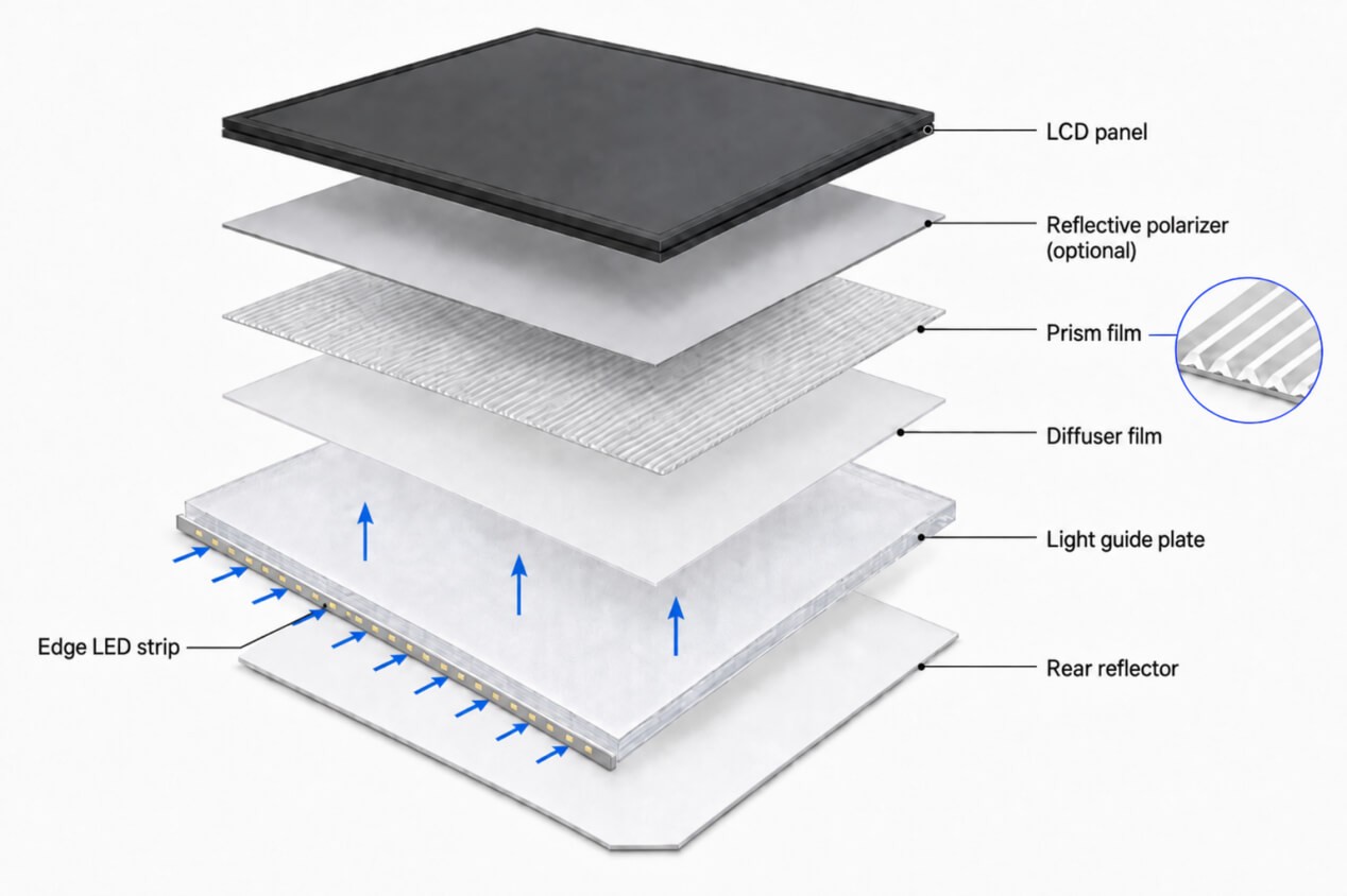
Above the light-distribution structure, optical films smooth brightness variations and direct more light toward the viewer. Each layer performs a distinct task:
| From the LCD toward the rear | Optical function |
| Reflective polarizer, when included | Returns otherwise unused polarization for recycling |
| Prism or brightness-enhancement film | Redirects light toward the intended viewing direction |
| Diffuser film or plate | Blends light and reduces visible source patterns |
| Light guide plate or direct-lit mixing space | Distributes illumination across the screen |
| Rear reflector | Returns backward-traveling light toward the panel |
Simplified stack; the number and arrangement of optical films depend on the backlight design.
A prism film improves on-axis brightness by redirecting light. A reflective polarizer such as DBEF instead recycles one polarization component, giving that light another opportunity to pass through the LCD’s rear polarizer. Combining these functions helps the module use its available illumination more efficiently.
Film orientation, cleanliness, and mechanical support must remain controlled during assembly. A misplaced or distorted optical sheet can introduce brightness patterns even when the LEDs and LCD cell are functioning correctly.
Adding Mini-LED and Quantum-Dot Enhancements
Some backlights extend this structure with local dimming or spectral enhancement.
Mini-LED local dimming divides the backlight into independently controlled zones. Adjusting those zones to match the image helps preserve bright highlights while reducing illumination behind darker areas.
A quantum-dot enhancement film (QDEF) changes the spectrum rather than the spatial brightness pattern. It converts part of the blue LED light into red and green wavelengths, supporting a wider color gamut when matched with the panel’s color filters.
These enhancements operate around the same core LCD structure. Once the backlight and supporting frame are integrated, the module is ready for complete electrical and optical evaluation.
7. Testing the Finished LCD Module
Inspection takes place throughout LCD manufacturing, but final module testing brings the electrical, optical, and mechanical results together. A panel that passed earlier checks can still develop a connection fault, trapped particle, or pressure-related defect during assembly.
Electrical checks verify pixel addressing and driver connections. Optical tests use solid colors, grayscale patterns, and other controlled images to reveal defective pixels, brightness variation, and color differences that complex video can conceal.
Identifying Mura and Its Causes
Visible unevenness is commonly described as mura. It can originate from variations within the liquid crystal cell, uneven backlight illumination, or mechanical stress introduced by the frame and other components.
The inspection stage helps narrow the cause. A pattern already present before backlight integration points toward a different problem than one that appears only after the frame is installed. Comparing results across production stages makes troubleshooting more effective than judging the finished image alone.
Some modules also use de-mura calibration, which converts measured brightness differences into correction data applied to the image signal. This can reduce correctable non-uniformity, but it cannot remove contamination or repair a broken electrical connection.
Checking Reliability Beyond the First Image
A clean image at room temperature is only part of the evaluation. Reliability testing examines how the module behaves under specified conditions such as elevated temperature, humidity, and thermal cycling.
These tests help expose weaknesses in bonds, seals, materials, and electrical connections that may not appear during a brief functional check. The results establish how the completed assembly performs beyond its initial power-on.
From LCD Module to Finished Digital Signage
An LCD module is not yet a complete digital signage unit. It still needs to be integrated with the control electronics, power system, enclosure, and any additional components required by the final application.
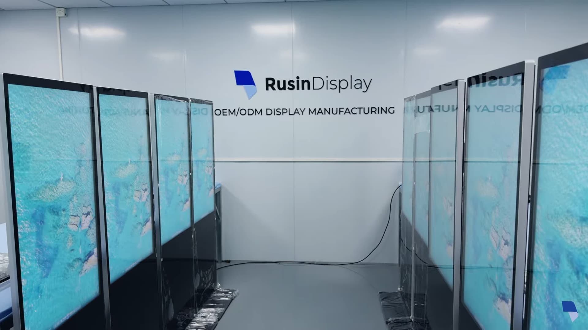
This downstream stage can be seen in a RusinDisplay production batch of several hundred LCD digital signage units prepared for shipment to Italy. The units moved through assembly and system integration, finished-unit inspection, and protective packaging before shipment.
Watch the RusinDisplay LCD digital signage assembly, inspection, and packaging process on YouTube.
At this stage, inspection covers the complete display rather than the LCD module alone. Image output, electrical operation, component connections, enclosure fit, and exterior condition are checked together before each unit is protected for transport.
From Glass to a Working Display
By the end of the LCD manufacturing process, large glass substrates have become individually addressed, color-filtered cells supported by driver electronics and a controlled backlight. The finished module is then integrated with a controller, power supply, enclosure, and any additional touch or protective components.
Its connection to the host electronics depends on the selected LCD display interface, while the surrounding mechanical and thermal design supports its operation in the final product.
The finished screen may look like a single surface, but its image quality comes from the alignment of many separate structures. Thin-film circuits, liquid crystal spacing, optical films, and electrical bonds all contribute to the clarity and consistency of what the viewer sees.
For your next commercial LCD display project, contact RusinDisplay to discuss your application and display requirements.
FAQ
How are LCD screens made?
LCD screens are made by forming thin-film circuits and color filters on glass substrates, sealing liquid crystal between them, and adding polarizers, driver electronics, and a backlight. Inspection throughout production checks that these electrical and optical structures work together correctly.
What is the difference between LCD panel fabrication and module assembly?
Panel fabrication creates the TFT circuits, color filters, and sealed liquid crystal cell. LCD module assembly adds the optical, electrical, and mechanical components needed to operate that cell, including polarizers, driver connections, a backlight, and supporting parts.
Is a finished LCD module ready to use as a monitor?
Not usually. An LCD module still needs compatible control electronics, power, and a suitable signal source. A complete monitor also adds an enclosure, external connections, and other system components.
Does LCD manufacturing automatically include a touchscreen?
No. Touch sensing is an additional function. Depending on the design, it can be integrated into the panel structure or added through a separate touch layer. TDDI combines touch-controller and display-driver functions, but a standard LCD module does not necessarily include touch capability.